 Solicon Cutting (Solar Cell)
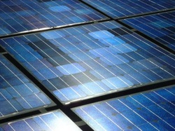
Silicon is widely used in a number of industries but primarily in solar cells and in semiconductor manufacture, with growing applications in jewellery and entertainment goods. In the majority of applications the source material is in the form of wafers which are typically 0.2-1.5mm (0.008”–0.06”) thick and 100-300mm (4”-12”) diameter. This application note focuses specifically on cutting of patterned wafer, single crystal, as well aspolycrystalline silicon(200µm). Looking at the both pulsed and CW lasers assessing their key competencies with silicon and the competitive edge fiber lasers have over all other existing silicon cutting technologies.
